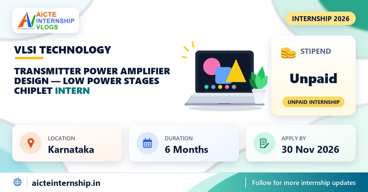
Applications are open for the VLSI Technology Transmitter Power Amplifier internship on the AICTE Internship Portal. It is unpaid, runs for 6 months and is based in Karnataka. VLSI Technology has 2 openings. Apply by 30 Nov 2026. VLSI Technology posted it on 16 Nov 2026.
The listing asks for B.Tech / B.E / equivalent. It suits students who want practical experience in design work. This post covers the work you will do, who can apply, the stipend, key dates and how to apply, with the official link. Details the listing leaves out are marked as not specified.
Internship Overview
Check these details before you apply.
| Organization | VLSI Technology |
|---|---|
| Internship Role | Transmitter Power Amplifier Design — Low Power Stages Chiplet Intern |
| Stipend | Unpaid |
| Location | Karnataka |
| Work Mode | Not specified |
| Internship Type | Full Time |
| Duration | 6 Months |
| Openings | 2 |
| Last Date to Apply | 30 Nov 2026 |
| Apply On | AICTE Internship Portal |

About VLSI Technology
No company profile is given in the listing. Check VLSI Technology's official website and LinkedIn page before you apply.
Internship Details
Transmitter power amplifier design low power stages chiplet within the SDR radio development programme.
- Work should connect the technical principles to the wider SDR system with attention to interfaces measurable performance documentation and verification wherever these are part of the module scope.
The expected outcome is a clearly documented contribution that can be reviewed and considered during system level integration.
Roles and Responsibilities
The listing describes the work like this:
The technical objective is to build practical understanding and implementation capability in this area. Development of low power transmitter stage design capabilities supporting 0.25W 1W and 2W output power levels through driver amplifier and pre driver stage design efficiency optimization and thermal management for the SDR radio PA chain.
- Study the module requirements and work through relevant engineering activities including PA chain architecture design frameworks supporting multi stage driver and final amplifier topology selection for 30 to 512 MHz wideband operation with selectable output power levels.
Driver amplifier transistor selection systems supporting gain linearity efficiency and frequency response trade off analysis for wideband 30 to 512 MHz driver stage design. Driver amplifier matching network design architectures supporting interstage matching between driver and final stage wideband matching using lumped elements or transmission line techniques and gain flatness across band.
You May Also Like: HQNCIW AI-Based RF Localisation Error Prediction Internship
Eligibility Criteria
The listing sets these criteria:
- Degree: B.Tech / B.E / equivalent
- You can work full time for the full 6 months

Required Skills
No specific skills are listed for this role.
Stipend and Benefits
No stipend is paid: the listing describes it as an unpaid internship. Decide whether the work experience is worth the time before you apply.

Benefits
- Hands on exposure to SDR receiver development and RF testing environments
- Practical training on industry standard RF test equipment and measurement instruments
- Experience in receiver sensitivity selectivity and performance verification
- Exposure to MATLAB Simulink Python and GNU Radio tools
- Opportunity to work on indigenous defence communication and SDR technology
- Internship completion certificate upon successful completion of the programme
- Opportunity to be considered for future employment based on performance technical skills and organisational requirements
Internship Duration and Mode
The internship runs for 6 months and is full time. The listing names Karnataka as the location. If you live elsewhere, check whether you can relocate for the full period.
Important Dates
| Posted On | 16 Nov 2026 |
|---|---|
| Last Date to Apply | 30 Nov 2026 |
| Internship Start Date | Not specified |
Required Documents
The listing does not list any required documents. Keep an updated resume in PDF format ready, as most forms ask for one.
Selection Process
The selection process is not described in the listing. Keep checking your email after applying, as shortlisted students are contacted there.
How to Apply
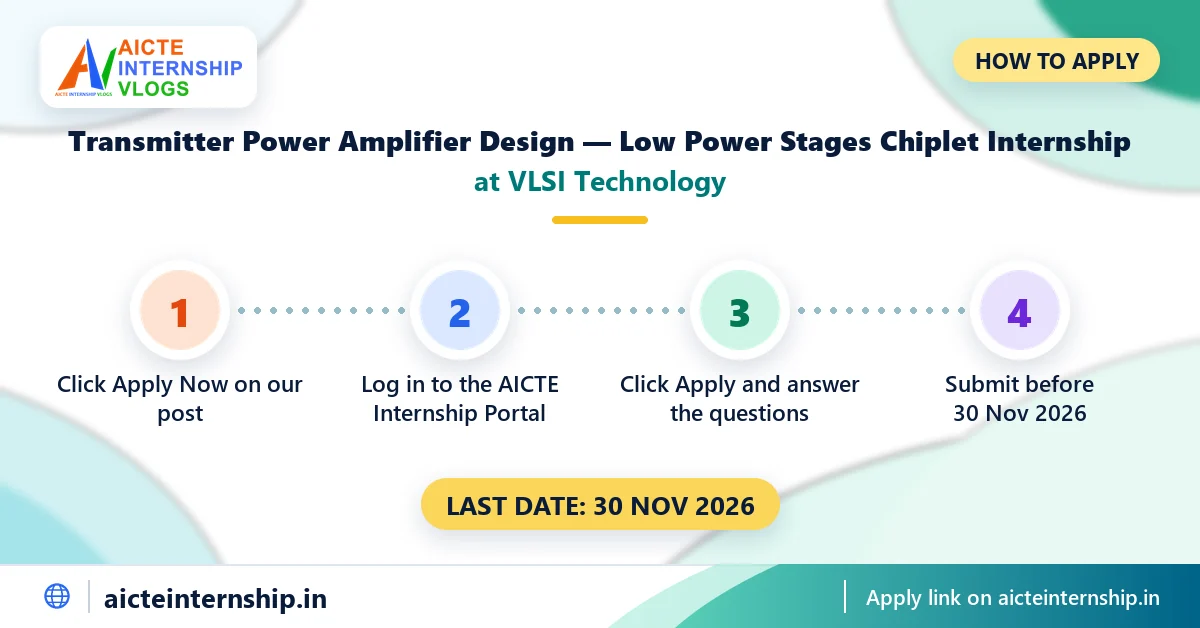
- Tap "Apply Now" below to open this internship on the AICTE Internship Portal.
- Sign in to the portal. First-time users need to register as a student.
- Read the details once more, then click Apply and answer the questions the company asks.
- Track your application status on your portal dashboard.
Important Official Links
- Official listing and application: Transmitter Power Amplifier Design — Low Power Stages Chiplet internship listing on the AICTE Internship Portal
- AICTE Internship Portal: internship.aicte-india.org
- VLSI Technology website: not given in the listing
The listing linked above has the complete description, which is shortened here.
Practical Tips for Applicants
- Complete your AICTE Internship Portal profile (college, course and year) before you apply, so the form goes through in one go.
- Keep a portfolio link ready (Behance, Dribbble or a PDF). Show 3-5 of your best designs.
- Match your resume to this listing: put the skills it asks for near the top.
- Apply a few days before the last date. Portals get slow near the deadline.
- Before an interview, spend ten minutes reading about VLSI Technology on its website and LinkedIn.
More Internships and Guides
Frequently Asked Questions
Short answers to what students usually ask about this role.
1How much does the VLSI Technology Transmitter Power Amplifier internship pay?
There is no stipend: the listing says it is an unpaid internship.
2Where is this internship located?
It is based in Karnataka.
3Who is eligible to apply?
It is open to students with B.Tech / B.E / equivalent.
4When does the application close?
The last day to apply is 30 Nov 2026. 2 students will be selected.
5How can I apply?
Open the listing with the Apply Now button, sign in to the AICTE Internship Portal and submit your application there.
6Will I get a certificate?
A certificate is given after you finish the internship.
7Is there any fee to apply?
The listing does not mention any fee. Genuine internships do not ask students to pay for selection.
Conclusion
This Transmitter Power Amplifier Design — Low Power Stages Chiplet role at VLSI Technology is a full time internship with no stipend, lasting 6 months. Check the official listing for any changes, then apply before the deadline.
About the Author
Disclaimer: This article is for information only. AICTE Internship Help Desk is an independent informational website and is not affiliated with AICTE or VLSI Technology. Check the latest eligibility, stipend, deadlines and application details on the official website before you apply.